VLSI

The Process/Technology Nodes
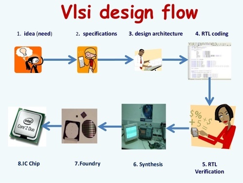
  • - Design Solutions from Specifications to GDSII sign-off for Analog, Digital and Mixed Signal chips, across process nodes from 350nm to most advanced 5nm
  • - Digital Design Turnkey Capabilities – RTL, DV, DFT, PD, till GDS sign off
  • - Analog/AMS Design Turnkey Capabilities – Analog Modelling, Circuit Design, Layout Design, AMS Verification
  • - Domain experience includes Data Converters, Power Management, High Speed Interfaces – PCIe, DDR, SerDes, SAS/SATA, Ethernet, MIPI, Foundation IPs etc

  • - Applications include Servers, Automotive, Graphics, Mobile platforms, Medical, Consumer products etc
  • - Expertise in Pre-silicon verification, FPGA Prototyping and Emulation
  • - Expertise in Post-silicon validation on Bench Char and ATE
  • - Expertise in Low power, High Power, High Speed designs with the knowledge and experience in power savings and design optimisation techniques

Our IC Capability Circuitry

Analog & Mixed Signal

Analog & Mixed Signal – The Highlights

  • - Complete Analog Design life-cycle from specs to post-silicon validation
  • - Expertise for developing Full IP & Block level
  • - Expertise on CMOS/FinFET process node: 5nm, 7nm, 10nm, 14nm, 22nm, 45nm, 65nm, 90nm, 130nm, 180nm & 350nm
  • - High Speed AMS Design & Layout
  • - RF Layout
  • - IO Design & Layout
  • - Standard Cell Design & Layout
  • - Verilog-A & V-AMS Modelling

RTL Design

Highlights

  • - Integration: Block integration, Clocks and Reset, Clock gating, DFT and DFD, Lint, CDC
  • - IP Block Development: Reusable, Pipelined, CDC, Lint, DFT, HW-SW partitioning
  • - Protocols: AMBA CHI/AXI/AHB/APB, MIPI (DSI, CSI, Slimbus, Soundwire, Unipro, NAND Flash); PCIe; SAS/SATA; SDIO Host/Device/Memory/Combo; I2C, SPI, UART, MDIO

Advanskills Systems Solutions

Advanskills Systems addresses the need for a system design and verification language that spans hardware and software. It is a language built in standard C++ by extending the language with a set of class libraries created for design and verification. Tessolve customers are applying Advanskills Systems for architectural exploration, performance modelling, functional verification, and high-level synthesis.

Design Verification

DV – The Highlights

  • - Flexible resources proficient in verification methodologies and tools.
  • - Tools for verification productivity
  • - Consultancy programs and continuous improvements through Benchmarking.
  • - Training on verification strategy and the latest verification methodologies.

Design For Test And Debug

DFT & DFD – The Highlights

  • - Multiple Clock and Voltage Domains
  • - Mixed signal low speed and high-speed designs
  • - Power sensitive designs
  • - Embedded processor-based designs
  • - Large number of memory types – SRAM, ROM, CAM etc.
  • - Complex Analog testing includes SERDES, DDR and A/D, D/A converters
  • - Experience in industry standard EDA tools for Memory BIST, ATPG, JTAG etc. from Mentor Graphics, Synopsys and Cadence
  • - Post silicon debug on ATE and Bench, demonstrating ownership from silicon architecture through silicon production

Physical Design

PD – The Highlights

  • - Experience in most advanced Process nodes down to 5nm.
  • - Integration of Analog & Mixed signal SOC
  • - Low Power design
  • - High Performance design
  • - Expertise on all industry standard EDA tools – Synopsys, Mentor, Cadence, Ansys etc.

FPGA Emulation and Post SI Validation

FPGA Emulation – The Highlights

  • - Tools expertise – Synthesis (Synolify Premier/Pro, Altera Tools), PAR & Timing Analysis (Xilinx & Altera Tools), Debug (Chip scope Altera Signal, Logic Analyzer, Oscilloscope, Trace 32)
  • - Simulation Tools – Modelsim, NCSIM, Questasim
  • Find us

    PO Box 16122 Collins Street West Victoria 07 Australia

  • Email us

    info@domain.com

    example@domain.com

  • Phone support

    + (066) 0760 0260

    + (057) 0760 0560